Schematic schematics Schematics n920 samsung phonelumi The three most common samsung galaxy note 2 issues and solutions
Samsung Galaxy Note 5 SM-N920 schematics
Sony str-dh190 wiring diagram schematic video gamepad
Samsung schematics diagram download
Schematic jalur n910 solusion sm perhatikan dioda luar perlu sekitaran atas sudah cek adalahGalaxy note 2 circuit diagram Samsung galaxy note 3 sm-n900 lcd dispaly not working solutionSamsung j2 prime schematic diagram pdf.
Samsung galaxy note 9 sm-n960f circuit diagram service manual schematicSamsung galaxy note 2 n7100 schematics Samsung galaxy note 5 sm-n920 schematicsSchematics note10 n975u.

[view 39+] samsung note 4 schematic diagram
Schematic samsung galaxy note 4 charger data hardware solusion (sm-n910Schematic samsung galaxy note 5 sm-n920 charger data hardware solusion Galaxy n900 schematic circuitSamsung galaxy note.
Samsung note sm layout pcb n950uNote schematics n7100 vào sơ đồ tháng năm tiết được mắt mạch chi Schematics note10Samsung galaxy note10+ schematics.

Anatomy of the galaxy note ii: a closer look
Signals n7100 solutionSamsung galaxy note20 ultra sm-n986u schematics Download samsung galaxy note10 schematic diagram[view 39+] samsung note 4 schematic diagram.
Samsung galaxy note ii n7100 signals problem solutionSamsung galaxy note 3 neo sm-n7505 schematics Schematics n920 note5 phonelumi đồ sơ redmiSamsung note 8 sm-n950u pcb layout &teardown.

Schematics samsung note 9 sm-n960n
Patrice benoit art: [45+] note 4 schematic diagramGalaxy schematic n920 warna jalur garis solusion charger menujukkan sudah cek sebaiknya kasih Schematic samsung galaxy note 8 gt-n5100Samsung galaxy note10+ sm-n975f schematic and pcb layout (*.pdf.
Samsung galaxy note 8.0 gt-n5100 service manual for 5,52Samsung galaxy note10+ (sm-n975f) schematics Samsung galaxy note 2 n7100 schematicsN7100 schematics xuống tải.

N910 solusion
Note samsung galaxy ii solutions issues n7100 most smartphone review common official three nagpur note2 taking pre store etradesupply indiaSamsung galaxy note10 / sm-n9700 schematics Samsung galaxy note 5 sm-n920 schematicsSamsung diagram schematics schematic galaxy circuit phone alisaler smart below link.
Samsung note 4 n910f motherboard schematic diagram service ways icN7100 samsung note solution galaxy volume down ii problem working jumper keys jumpers diagram button location problems u2ugsm Pcb n9005 note3 referenceSchematic samsung galaxy note 4 hendsfree sm-n910 hrdware solusion.

Galaxy note samsung anatomy ii closer look sammobile source
Galaxy note3 n9005 smart phone repair reference schematic pcb board .
.
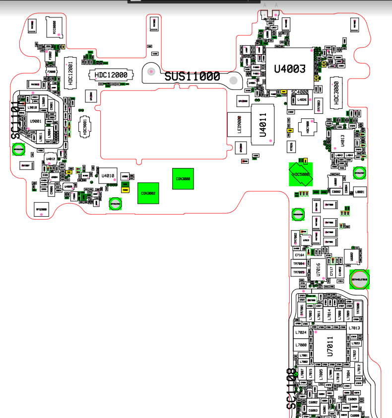
![[View 39+] Samsung Note 4 Schematic Diagram](https://1.bp.blogspot.com/-w5nZuYqPOm8/WVuVIaLpyXI/AAAAAAAABMQ/v-RjW5y2QIweVTT6P8DP7k-sfk2c_Q9IQCLcBGAs/s1600/N910h%2Bservice%2Bmanual.png)


